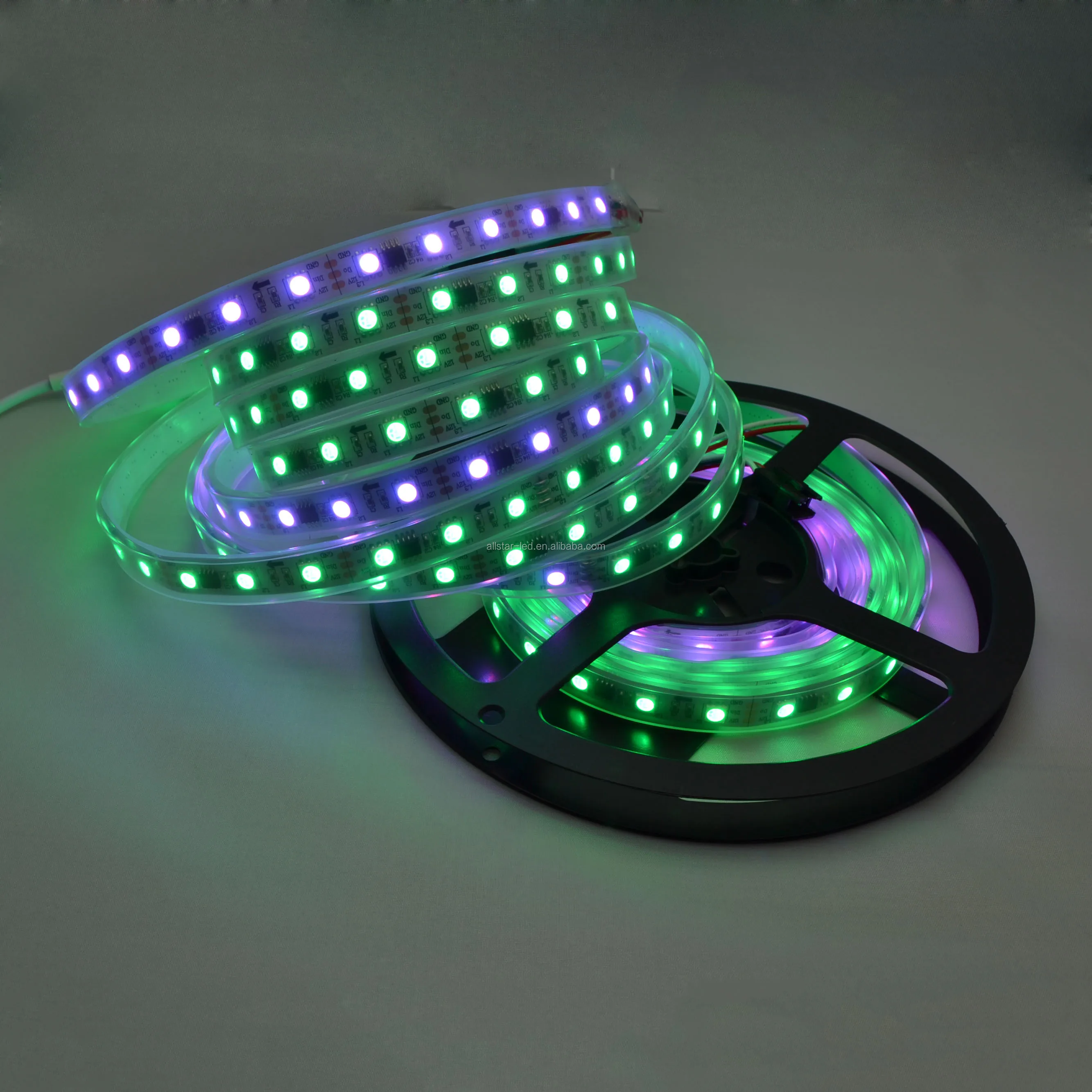
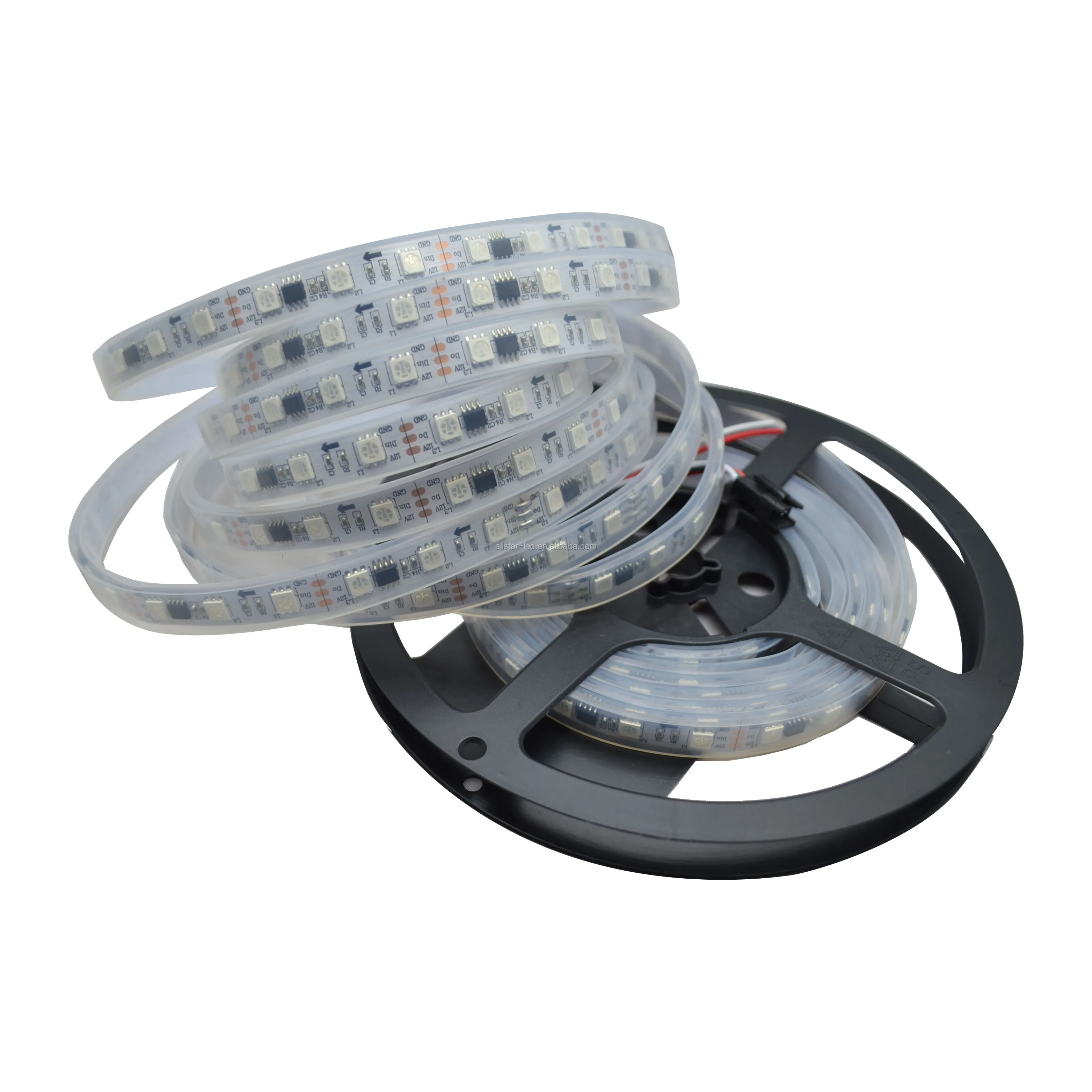
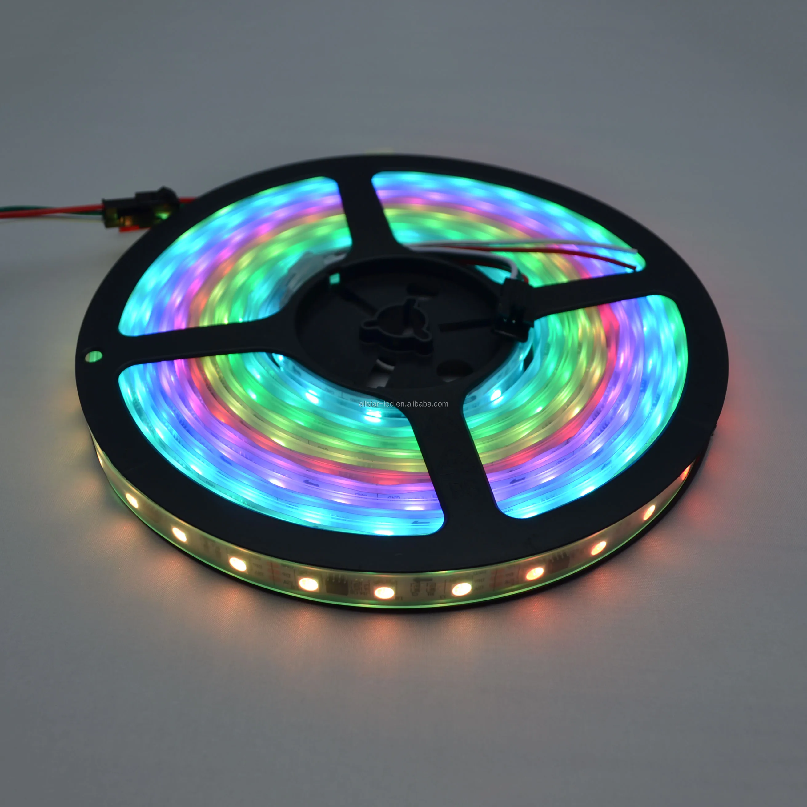
Addressable Ws2811 Rgb Led Strip Light 5050 12v 5m 60 leds/m Digital Rgb Led Tape
Spec
5050 smd rgb led strip ws2811
Input voltage :.............DC12v;
Power: .......................14.4watt/meter, 72watt/roll;
LED resource:.............High brightness 5050 RGB;
Q'ty of LED: ...............60leds/meter, 240leds/roll, each 3LEDs separately controlled
IC Type: .....................ws2811 IC;
Q'ty of IC: ..................20IC/meter (1 IC drives 3led chip);
Pixels:.........20/meter;
Pitch: .........................16.6mm(1000/60);
Grey scale: ................256;
Bits/color: ...................8-bits/each color;total 24 bits for RGB
FPC size: ....................Width: 10mm, High: 2.5mm;
FPC color: .................white
Protection rate: .......... waterproof in silicon tube
Colors: ........................Full color RGB, dream color changing;
Cuttable:......................every 3LEDs cuttable;
Package: ....................5meters/reel in anti-static bag.
Control System
Compatible with Arduino and DMX512.
Installation
3M adhesive tape for IP40 and IP65;
3M adhesive tape or Silicone IG-K and screw for IP67;
Silicone IG-K and screw for IP68.
Ws2811 ic chip main spec:
Output port compression 12V.
Built in stabilivolt, Only add a resistance to IC VDD feet when under 24V power supply.
Gray level 256 can be adjusted and scan frequency not less than 400Hz/s.
Built in signal reshaping circuit,after wave resha-ping to the next driver, ensure wave-form distor-tion not accumulate.
Built-in electric reset circuit and power lost resetcircuit.
Cascading port transmission signal by single lin-e.
Any two point the distance more than 10m tran-smission signal without any increasecircuit.
When the refresh rate is 30fps, low speedmodelcascade number are not less than 512 points, hig-h speed mode not less than1024 points.
Send data at speeds of up to 400 Kbps and 800Kbps two patterns.
General description
The WS2811 is 3 output channels special for LED driver circuit. It internal include intelligent digital portdata latch and signal reshaping amplification drive circuit.Also include a precision internal oscillator and a 12V voltage programmable constant current output drive. In the purpose of reduce power supply ripple, the 3 outp-ut channels designed to delay turn-on function.
IC use single NZR communication mode.After the chip power-on reset, the DIN port receivedata from controller, the first IC collect initial 24bit data then sent to the internal data latch, theother data which reshaping by the internal signal reshaping amplification circuit sent to the next cascade IC through the DO port. After transmission for each chip,the signal to reduce 24bit. IC adopt auto reshaping transmit technology, making the chip cascade number is not limited the signal transmission, only depend on the speed of signal transmission.
The data latch of IC depend on the received 24bit data produce different duty ratio signal at OUTR, OUTG, OUTB port. All chip synchronous send the received data to each segment when the DIN port input a reset signal. It will receive new data again After the reset signal finished. Before a new reset signal received, the control signal of OUTR ,OUTG, OUTB port unchanged. IC sent PWM data that received justly to OUTR, OUTG, OUTB port, after receive a low voltage reset signal the time retain over 50us. We offer two package SOP8 and DIP8.


