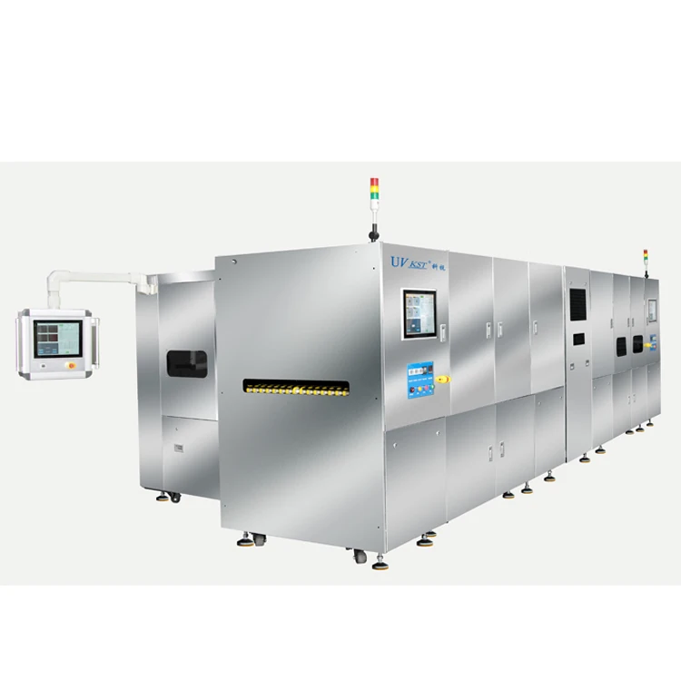
Homepage|Business Center|Save the Page|Get the App
普通会员

Dongguan KST Automation Technology Co., Ltd.

Product Category
  • No Category Yet
Search
 
Link
  • No links
Home > Products > AUTO OUTER LAYER COLLIMATED UV EXPOSURE SYSTEM PCB Manufacturer China
AUTO OUTER LAYER COLLIMATED UV EXPOSURE SYSTEM PCB Manufacturer China
Click on the image to view the original image
Product: views:3AUTO OUTER LAYER COLLIMATED UV EXPOSURE SYSTEM PCB Manufacturer China 
Unit Price: Negotiated
Min.Order:
Supply:
Delivery: Shipment within days since the date of payment
Valid until: Long Term
Updated on: 2020-12-03 09:53
  Negotiated
Product Details
Product Description
AUTO OUTER LAYER COLLIMATED UV EXPOSURE SYSTEM PCB Manufacturer China
Automatic Outer layer exposure machine
Features:
1.For Outer Layer
2.Usability for 0.1mm thickness Panel
3.High Throughput Cycle Time = 13 sec + Exposure Time
4.High Resolution L/S 50μm/50μm
5.Alignment accurancy ±12.5um/±0.5mil
6.LED Light Instant ON/OFF, Reduce Energy Costs.(Lift time better than Mercury UV-LAMP)
7 Non-contact magnetic Roller Prevented Particle Occur
8Precise and Speedy Linear Servo Transfer for Sucking System
9 Adjustable Vacuum-Pad To Fit The PCB With High-Speed
10.Temperature and Humidity Control Units
  • LED Light source

1. LED light source, energy saving, lowest cost and power consumption, no replacement consume during three years.
2. KST own design LED lght source,easy maintain and replace.
3. Long service life, >20,000 hours, and maintain for three years.
Model
KST-AEM6457-WX
Circuit Board size
Min:10"*12"
Max:24.5"*28.5''
Circuit resolution
2mil/2mil
Energy Uniformity
≥88%
Exposure time
100% energy<8s
Adjustable
Time and energy can be adjust
PCB thickness
0.1mm-3.2mm
Detailed Images
For outer layer,single side
-Alignment Precision ±12.5um/±0.5mil
-Multiple Wavelength UV-LED
Packing&Shipping
After Sales Service
询价单
total0items  Comments