


 Share
Share


Brand: |
none |
Address: |
China |
Min.Order: |
none |
Supply: |
none |
Valid until: |
Long Term |
Product Details
| Attribute | Measurements |
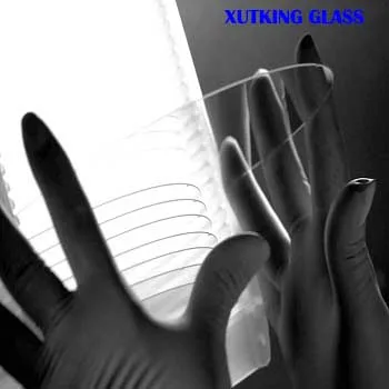
Diameter | Φ2",Φ3",Φ4",Φ5",Φ6",Φ8",Φ12" |
Thickness | 0.2mm,0.3mm,0.4mm,0.5mm,0.7mm,1.0mm,1.5mm tolerance±0.02mm) |
Dimensional Tolerance | +/- 0.02 |
Thickness Tolerance | +/- 5μm |
Thickness Variation (TTV) | < 0.01mm |
Flatness | 1/10 Wave/Inch |
Surface Roughness (RMS) | <1.5nm |
Scratch and Dig | 5/2 |
Particle Size | <5μm |
Bow/Warp | <10μm |
The following describes the versatility within several of our key processes. For full details on the process, please contact us freely get more information.
WAFER FABRICATION PROCESS
Shape Cut
Thin sheets are scribed, thick sheets are water jetted and blocks are wire sawn to begin the process with a wafer “blank”.
CNC Edge
Each wafer is individually edged on a Precision CNC Edge Grinding Station.
Lapping
As required, wafers are lapped to precise thickness or flatness.
Polishing
Double-side Commercial Polish removes subsurface damage and Super Polish creates a pristine finish.
Cleaning
We combine ultrasonics and megasonics on multiple cleaning lines which feed directly into a Class 100 Clean Room.
Inspection
In our Class 100 Optical Clean Room, we inspect to various quality levels under the appropriate lighting conditions.
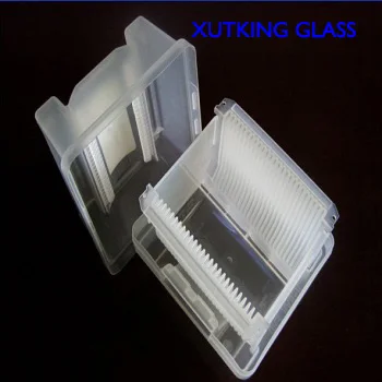
Packaging
All wafers are packed in pre-cleaned containers, double bagged and vacuum sealed within the Class 100 Clean Room.

WAFER SPECIFICATIONS
Tking produces wafers to all SEMI Standards including dimensional, flat and notch specifications. In addition, we offer custom specifications designed to your unique needs including, alignment marks, holes, pockets, edge profile, thickness, flatness, surface quality, cleanliness or any other details critical to your application. We also offer these wafers in a broad array of materials including Borosilicate, Aluminosilicate, Fused Silica (instead of quartz), Quartz and Soda Lime.
Customer Reviews total 0 items