Dongguan KST Automation Technology Co., Ltd (KST) is a national new- and high-technology enterprise that researches and develops, produces, sells, and services auto and semi-auto LED exposure equipment. The Company has three major subsidiaries, Dongguan Rsee Lighting Technology Co., Ltd., Dongguan Kerun Intelligent Technology Co., Ltd., and Dongguan KST Software Technology Co., Ltd. In 2017, KST acquired Japanese enterprise Rsee Lighting Technology Co., Ltd.Enhance its technological prowess in optical design, light source research and development. In November of the same year, Dongguan Kerun Intelligent Technology Co., Ltd. was established as part of the effort to pursue the strategy of backward integration to control raw material costs and keep the prices stable; also in 2017, KST passed acceptance inspections for provincial projects of industry-university-research institute collaboration and for projects funded by provincial innovation funds. Committed to the R&D, production and sale of LED exposure machines, the Company, by importing foreign advanced optical technologies and targeting the actual needs of domestic and international PCB industry, has managed to made its own technological innovations, and has applied for 12 invention patents, 46 utility model patents, and 9 design patents; except for 3 invention patents, all other 64 patents have been granted with corresponding certificates. The Company is successful in developing high performance full-automatic LED exposure machine and other high-end equipment that lead in performance in China. Now KST is selling its products around the world, with its most clients in the United Kingdom, South Korea, the Philippines, India, Slovenia, Ukraine, and Vietnam. Included in the major domestic clients are Ellington in Zhongshan, Eleceltek, Techwise, and Fastprint. KST has made a long term strategic plan that the Company will focus on Dongguan and expand its operations in the world, and that it will try to make KST-branded LED exposure systems the benchmarks of the industry. KST's research team will work relentless to reduce energy consumption and pollution for our clients, and to contribute to the society.
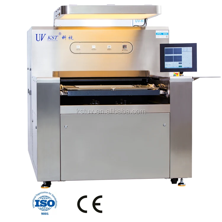
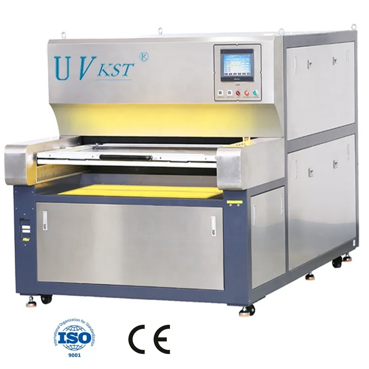
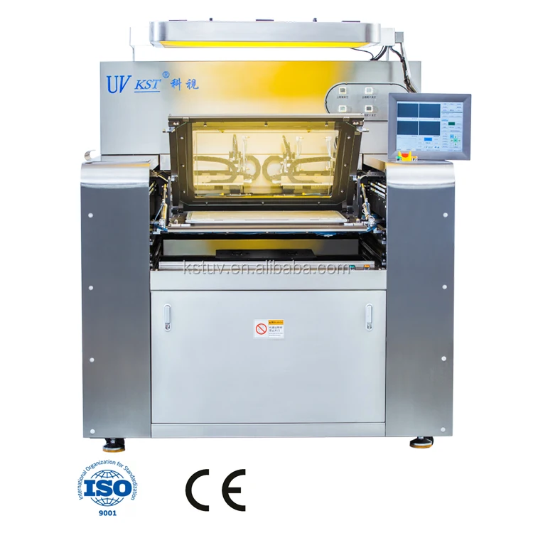
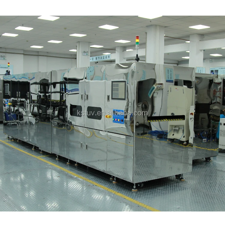
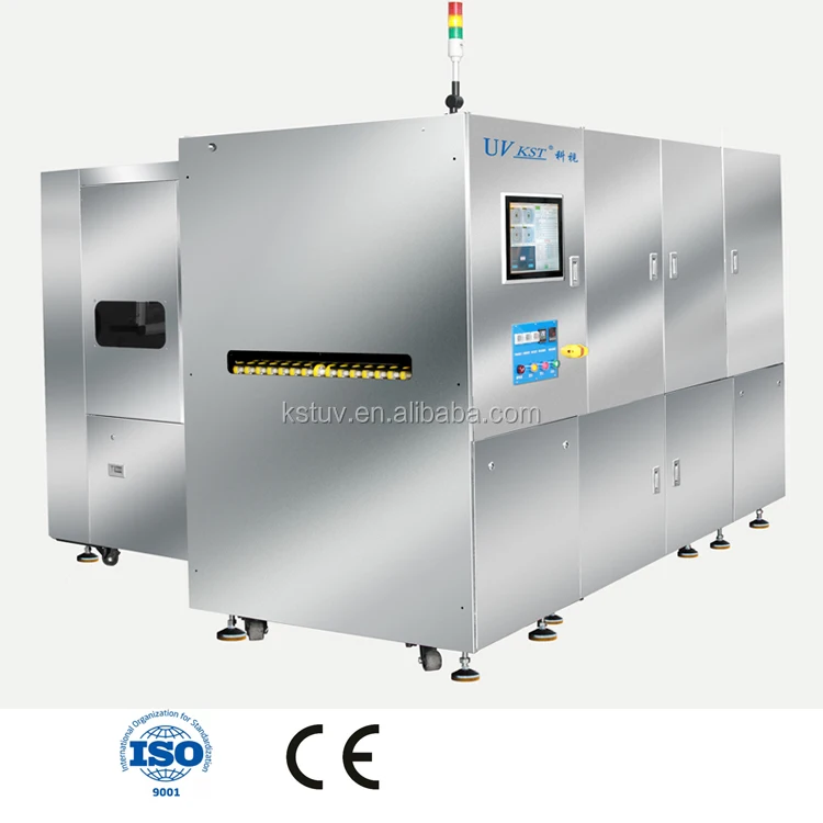
Multi layer inner layer mobil phone circuit LED PCB panel UV exposure machine
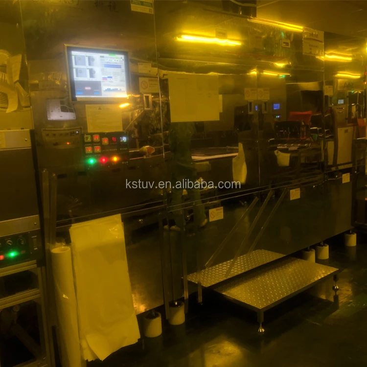
Inner layer PCB Exposure
Features:
-For Inner-Layer Liquid -High Resolution width/sapce 50μm/50μm -High Throughput Cycle Time = 10sec + Exposure Time -Scan light -A/W Alignment Precision 3σ≤ 10μm -LED Module Gain Control & Status Monitoring -LED Module Off-Line Monitoring Irradiance Distribution -LED Light Instant ON/OFF, Reduce Energy Costs. (Lift time better than Mercury UV-LAMP)
LED Light source
1. LED light source, energy saving, lowest cost and power consumption, no replacement consume during three years.
2. KST own design LED lght source,easy maintain and replace.
3. Long service life, >20,000 hours, and maintain for three years.
4. Automatic energy calibration and compensation, uniformity can automatic calibration to above 90% 5. Achieve the best green ink bridge, through multi wavelength.Undercut≦0.6mil(on copper surface ) 6. Production speed: 5~5.5 panel/min
Model
KST-AEM6457-NX
Circuit Board size
Min:12"*12" Max:21.5"*24.5''
Circuit resolution
2 mil/2mil
Energy Uniformity
≥90%
Exposure time
100% energy<3s
Adjustable
Time and energy can be adjust
PCB thickness
0.1mm-3.2mm
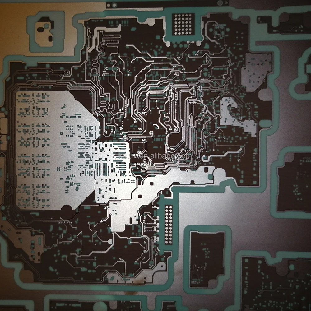
Detailed Images
For inner layer circuit. -Alignment accuracy: 12.5um±0.5um -Multiple Wavelength UV-LED


 Share
Share


Customer Reviews total 0 items