

 Share
Share


Western Europe 30.00%
South Asia 20.00%
North America 20.00%

China
Long Term
2020-12-17 13:14


Brand: |
none |
Address: |
China |
Min.Order: |
none |
Supply: |
none |
Valid until: |
Long Term |
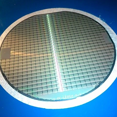
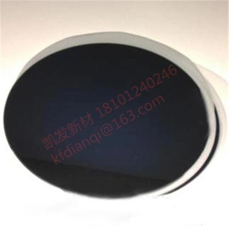
Double side polishing single crystal silicon
Specifications:
Single crystal, 4 inches*0.5mm. Transmission wavelength is 1200-14000nm. Double side polishing, in spot.
Material:
High purity silicon Si single crystal substrate. N/P optional.
Resistivity:
0.0001-100 Ω.
Growth mode | straight, pull |
Crystal orientation | [111]/[100]/[110] |
Flatness | <1 microns |
Surface roughness | about 5 |
Uses:
1.PVD/CVD coating substrate
2.used as XRD (X ray diffraction analysis), SEM (scanning electron microscope), AFM (atomic force microscope), FTIR infrared, fluorescence spectroscopy and other analytical test substrates
3.synchrotron radiation experimental sample carrier
4.substrate for molecular beam epitaxial growing
5.semiconductor lithography process, and so on

Customer Reviews total 0 items